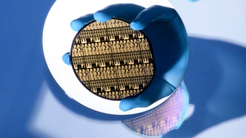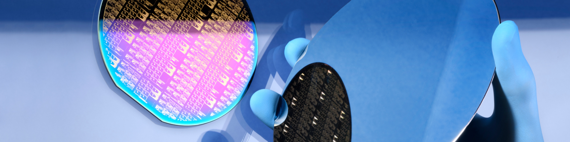
Photonic Chip Pilot Line: InP chip fabrication at 6-inch wafer scale
The Netherlands is developing a new industrial pilot line for photonic chips. This pilot line, hosted by TNO and part of the EU’s PIXEurope project, will be built at the High Tech Campus Eindhoven starting January 2026. Once operational, it will serve as a testbed and fab to facilitate full-scale manufacturing of advanced Indium Phosphide (InP) photonic chips at a 6-inch wafer scale. By combining research and manufacturing, the pilot line will help turn innovative ideas into cutting-edge real-world technologies - faster, energy efficient, more reliable and at scale.

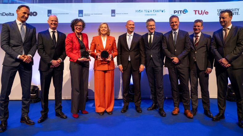
‘This photonic chip pilot line is a game-changer for Dutch companies and the future earning power and prosperity for the Netherlands. It is a critical part of a powerful PhotonDelta ecosystem with which the Netherlands can distinguish itself worldwide.’
To make photonic chips widely available, they need to be produced at scale – and that’s where the pilot line comes in. It’s designed to bridge the gap between research and industrial manufacturing, focusing on InP photonic chips. At a 6-inch wafer scale, the pilot line can produce many more chips per wafer, making industrial-scale production more efficient and cost effective. This step is crucial for turning bright ideas into practical technologies that can be used in everyday products and systems.
Serving tomorrow’s technologies
Pilot lines play a vital role in turning new technologies into real-world solutions. They allow engineers and companies to test how production performs under realistic conditions – before scaling up. This pilot line will help reduce risks by providing valuable insights into how InP photonic chips behave when produced at 6-inch wafer scale. It will also help assess technical feasibility, production costs, and market readiness. The pilot line ensures that innovations are validated and demonstrated in environments that closely resemble actual industrial settings.
Once operational, the pilot line will give companies a powerful boost in developing next-generation photonic chip technologies. It will speed up prototyping, support the launch of new startups, and help scale promising innovations into real-world products. TNO will host the facility for five years, after which it may be transferred to industry as a full-scale production site.

‘We are thrilled to engage in this much-needed ecosystem initiative, which will strengthen our ability to serve our customers in all markets even better. By scaling up together, we ensure this collaboration strengthens our leading position in the Netherlands and across Europe.’
PhotonDelta ecosystem
The pilot line is a joint effort by leading Dutch organizations. Startups, SMEs, and established companies will use the facility to develop and scale up their products in the InP photonic chip domain. As a European leader in InP technology, SMART Photonics is, next to others, an important knowledge provider and end user of the pilot line. In addition, the company serves as a training provider, helping to build the skills and knowledge needed across the ecosystem.
On the research side, TNO, Eindhoven University of Technology, and the University of Twente are working together within the jointly founded Photonic Integration Technology Centre (PITC). PITC combines deep expertise in photonic design, development, and industrialisation, and has helped many companies in developing products for photonic chips. The pilot line will be built at High Tech Campus Eindhoven — a European hotspot for integrated photonics and home to the vibrant PhotonDelta ecosystem of startups, scale-ups, and research organisations.
PIXEurope: a European initiative
PIXEurope is a major European programme under the Chips Joint Undertaking (Chips JU). The long-term goal is to establish the world’s first fully integrated, open-access pilot line for photonic chips right here in Europe. The Eindhoven pilot line is part of PIXEurope and is funded through the EU Chips Act, PhotonDelta, TNO, the Ministry of Economic Affairs, and the Ministry of Defence.
PIXEurope brings together leading research organisations and industrial partners to address key technological and production challenges across the entire photonic chip supply chain. This includes advanced chip fabrication, materials integration, packaging, and testing. The programme also supports the integration of photonic and electronic circuits, paving the way for next-generation semiconductor systems and strengthening Europe’s position in this critical technology field.
Career opportunities
Join the pioneering team at Europe’s first full-scale pilot line for advanced InP photonic chips at High Tech Campus Eindhoven, and help accelerate a key enabling technology with leading Dutch companies and world-class research institutes.
A strategic asset for Europe
Photonic chips — also known as Photonic Integrated Circuits — are tiny circuits that use light instead of electricity to transmit data. This makes them faster, more energy efficient, and ideal for powering the technologies of tomorrow. From AI and quantum computing to 6G networks and advanced medical diagnostics, photonic chips are at the heart of innovation. Their ability to handle massive amounts of data at high speed with minimal energy use makes them perfect for smart sensors, autonomous systems, secure communications, and high-performance computing.
Photonic chips aren’t just a promising technology — they’re a strategic asset. They play a key role in enabling Europe’s leadership in key enabling technologies like AI, quantum, and secure communications. Integrated photonics is one of the priority key enabling technologies within Dutch National Technology Strategy. By developing this pilot line, the Netherlands strengthens its position as a European hub for photonic innovation and manufacturing. It also helps reduce Europe’s reliance on global supply chains, which have proven vulnerable to recent geopolitical tensions and disruptions. This initiative supports both technological sovereignty and economic resilience.
The pilot line targets European industrial end-users, system integrators, startups, SMEs, and research institutes working on scalable InP photonic integrated circuits (PICs). It connects foundries and IDMs to OSATs, training providers, and material suppliers. While focused on European collaboration, international partnerships with Japan, Taiwan, and South Korea are also planned.
The pilot line supports advanced applications across multiple sectors, including AI, 6G networks, quantum computing, medical diagnostics, climate monitoring, and defense systems. Indium Phosphide (InP) photonic chips produced on the line offer high speed, low energy consumption, and large bandwidth, making them ideal for data centers, smart sensors, secure communications, and high-performance computing.
Scaling from 4- to 6-inch wafers increases production efficiency and chip yield, making industrial-scale manufacturing of photonic chips more viable. It’s a key step toward cost-effective, high-volume deployment of advanced photonic integrated circuits (PICs). The shift also aligns with semiconductor industry standards, enabling better integration with existing manufacturing infrastructure.
Unlike a standard manufacturing line focused on high-volume output, the pilot line combines R&D and manufacturing. It enables companies to test, validate, and fabricate new photonic chip designs using industrial-grade processes without committing to full-scale production. This reduces risk, accelerates innovation, and supports ecosystem-wide collaboration.
The pilot line enables companies to test and implement complex technologies that would be too costly or risky to develop alone. It helps companies validate new concepts and transfer them smoothly into production, offering clarity on required devices and conditions for optimal product development. Instead of shelving ideas due to technical barriers, the pilot line turns innovation into reality, accelerating hardware prototyping for research institutes, startups, and SMEs. By enabling low-volume production of InP photonic chips at 6-inch wafer scale, a leap from the current 3–4 inch standard, it strengthens the competitiveness of the Dutch PhotonDelta ecosystem. The line supports innovation, shortens time-to-market, attracts investment, and positions the Netherlands as a European leader in photonic chip technology.
As a key R&D and industrialization partner, PITC (Photonic Integration Technology Centre) plays a key role in bridging research and industry. It helps companies design, test, and scale their own photonic integrated circuits (PICs) using the pilot line’s 6-inch wafer platform. Through PITC, Eindhoven University of Technology (TU/e), the University of Twente (UT), and TNO contribute deep expertise in photonic design, development, and scaling. Its expertise ensures that new technologies can be industrialized efficiently, helping to strengthen the Dutch and European photonics ecosystem.
As a European leader in InP technology, SMART Photonics is, next to others, an important end user of the pilot line and as such can help accelerate industrial adoption and strengthen the Dutch photonics manufacturing base. SMART Photonics supports the pilot line with its proven expertise in Indium Phosphide (InP) technology to accelerate the development of processes for 6-inch wafer production by sharing skills and knowledge. In addition, the company serves as a training provider, helping to build the skills and knowledge needed across the ecosystem.
The pilot line is part of the EU’s Chips for Europe Initiative, which aims to bridge the gap between lab innovation and industrial production. This initiative supports the development of advanced technologies, like photonic chips, by offering facilities to test, scale, and validate prototypes. As part of PIXEurope, one of five pan-European pilot lines co-funded by the Chips Joint Undertaking, the pilot line in Eindhoven contributes to Europe’s technological sovereignty and global competitiveness.
Construction of the pilot line will begin in January 2026 at the High Tech Campus in Eindhoven. It is expected to become operational in 2027. Once running, the facility will serve as a testbed and fab for Indium Phosphide (InP) photonic chips at 6-inch wafer scale, supporting the transition from research to industrial production. Meanwhile, early collaboration opportunities are already available and will be further developed as part of the pilot line. The first inquiries have already been received.
The pilot line in Eindhoven is funded through the EU Chips Act by the Chips Joint Undertaking and co-financed by PhotonDelta, the Dutch Ministries of Economic Affairs and Defense, and TNO. The total investment amounts to 153 million euros over five years. Additionally, the High Tech Campus Eindhoven is investing in the building and the cleanroom.
Funded by the European Union
Views and opinions expressed are however those of the author(s) only and do not necessarily reflect those of the European Union or ChipsJU. Neither the European Union nor the granting authority can be held responsible for them. The acquisition and operation of the Chips JU Pilot Line is funded jointly by the Chips JU, through the European Union’s Digital Europe programme and Horizon Europe programme, as well as by the Participating States.
Co-funded by


Partners

End users
Contact us
-

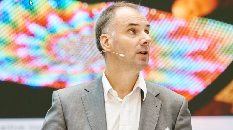
Jos van den Broek
Functie:Director Photonic Chip Pilot Line-
Standplaats:Eindhoven - Holst Centre
-
Email:Email Jos
-
Get inspired
Industrial photonic chip factory in Eindhoven launched
Construction start event: Dutch Photonic Chip Pilot Line
Gerwin Gelinck Honorary Professor Integrated Photonics at the University of Twente
Time setter story: Boudewijn Docter

TNO signals start of photonic chip pilot line