TNO Semicon Event 2026: Building bridges to reach Moore
We aim to drive technological progress and foster collaboration within the international semiconductor ecosystems. We strive to bring together corporates, start-up companies, innovators, and policymakers to share knowledge, engage in discussions, and advance the industry.
- Startdatum:
- Time:
- 09:00 - (CET)
- Location:
-
Conference Center, High Tech Campus 1-B, The Strip, 5656 AE Eindhoven
Building Bridges to Reach Moore
In 2026, the semiconductor industry faces mounting challenges. Demand for computing power is accelerating like never before, fueled by AI applications, edge computing, and the pursuit of sustainable materials and processes. At the same time, geopolitical tensions, resource scarcity, and the drive for energy efficiency are prompting the sector to actively engage in collaborations, often with new international partners. Achieving the next generation of chip technology demands strong connections between countries, research institutes, and companies. In this rapidly evolving landscape, we invite you to join us at the TNO Semicon Event 2026: ‘Building Bridges to Reach Moore’.
Programme
Walk-in, registration & innovation market
Coffee, informal networking & Innovation market with TNO technologies & start-up companies
Welcome & opening
Lisa Burke, Moderator of the day & Rogier Verberk, Director of TNO Semicon & Quantum

Keynote
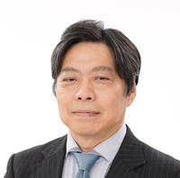
Junichi Tanaka, Hitachi Hightech Company
Keynote
Christina Porter, Invisix

Pitches of TNO researchers
Topics: AI and Acoustic Metrology
Keynote
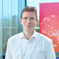
Johan Feenstra, Smart Photonics
Pitch
Jelle de Jong, FononTech
Wrap-up & closure
Lisa Burke and Rogier Verberk
Lunch break
Networking & Innovation market
Parallel Breakout sessions in two rounds
Technology deep dives from TNO experts and start-up companies
- 13:30 – 14:15: Round 1
- 14:45 – 15:30: Round 2
Networking drinks
Networking with refreshments.
Get to know the speakers
Christina Porter is a co-founder and CEO of Invisix Measuring Systems, an Eindhoven based semiconductor metrology startup developing next-generation soft x-ray scatterometry instruments for advanced logic and memory nodes. She holds a PhD in physics and has spent the last 12 years working on short wavelength metrology, pairing high harmonic generation sources with advanced inference algorithms for critical dimension and overlay metrology. Prior to founding Invisix, Christina worked for 7 years in project leadership and pathfinding for the ASML soft x-ray metrology program. This technology, developed for 10 years at ASML, was licensed to Invisix in 2026 enabling continued development externally. Christina holds 16 published patents and her academic publications have received over 850 citations.
Johan joined SMART Photonics as CEO in 2019, after having served on their Advisory Board for about 3 years. At SMART, he has raised € 150M with his team to grow SMART Photonics to become a globally leading foundry in the integrated photonics industry.
Johan is currently part of the Semicon Board NL, chairing a European focus group of 8 CEO’s and part the 10 Tech Champions, representing the Dutch National Technology Strategy.
Before SMART, Johan co-founded Liquavista in 2006 and is co-inventor of electrowetting displays. At Liquavista, he had a broad set of roles, ranging from CEO, to CTO and Director Program Management. Together with his team, he raised four rounds of venture capital for Liquavista and sold the company twice, in both cases to Fortune 500 companies (Samsung Electronics and Amazon.com). Johan is also serving as an advisor and/or supervisory board member for a number of start-ups and scale-ups.
Johan received his PhD in Solid State Physics from the Rijksuniversiteit Groningen in the Netherlands in 1997.
Junichi Tanaka is the Senior Chief Strategist at Hitachi High Tech Europe and holds a Doctoral degree in Engineering. His career has centered on advancing the monitoring and control of semiconductor fabrication processes, from developing plasma simulators and etcher monitoring tools to pioneering plasma spectral CT for analyzing in chamber plasma distributions and introducing FTIR based diagnostics for stabilizing plasma processes. These efforts deepened the understanding of plasma etching and led him to implement fab wide APC systems driven by CD SEM based feedback control, earning the Semicon Japan Technology Symposium Award in 2008.
Today, his work focuses on next generation metrology and inspection technologies, including time domain laser and electron beam techniques. He emphasizes the need for higher resolution CD SEM as semiconductor processes continue to scale, while driving innovations to enhance in line metrology performance and introduce new inspection modalities.

Register for TNO Semicon Event 2026
Register now to secure your place at the TNO Semicon Event 2026 on 15 April. Join industry, research, and policy leaders shaping the future of semiconductors.
Contact us
-
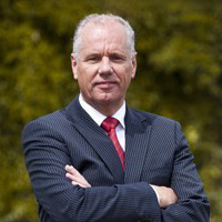
Rogier Verberk
Functie:Director Semicon & QuantumDr Rogier Verberk holds a PhD In experimental physics from Leiden University (2005). At TNO, the Dutch national Research and Technology Organisation, Rogier worked on EUV lithography with ASML and Carl Zeiss and became principal project manager.
-
Standplaats:Delft - Stieltjesweg
-
Email:Email Rogier
-
Get inspired
Quantum internet and quantum networks series 1.0

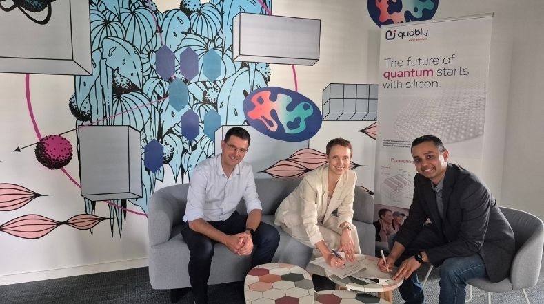
TNO and Quobly join forces to advance industrial-scale silicon quantum technology
Pioneering with a purpose: The Netherlands at the forefront of quantum innovation
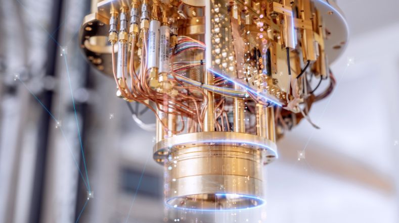
Pioneering on the edge of physics: quantum chips tested faster and faster
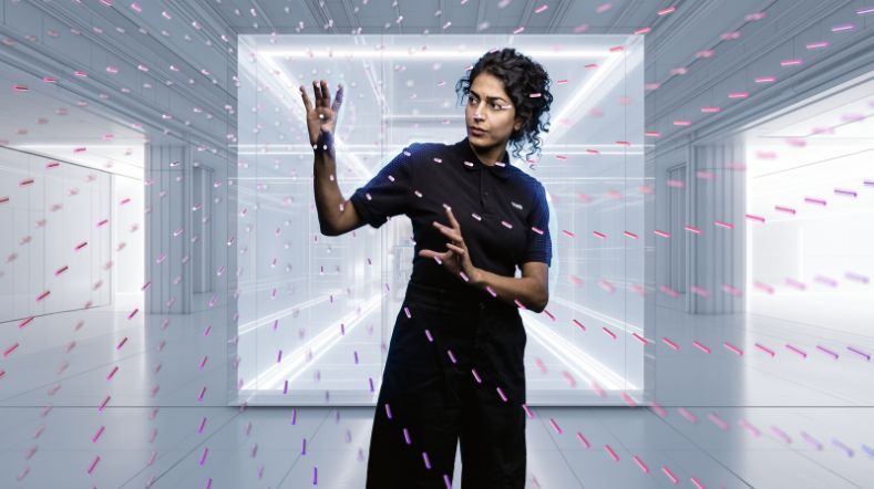
How TNO’s Ines Corveira Rodrigues shapes tomorrow's quantum world
