Ready to shape the future of photonic chips?
This is the time to work on a faster, more reliable and accessible manufacturing ecosystem for the fabrication of advanced photonic chips. This strengthens Dutch industry and reinforces Europe's position in photonic innovation. We’re at a pivotal moment as focus will be shifting from groundbreaking research to large-scale industrial manufacturing. Now, we’re looking for pioneers ready to build something new in this fast-evolving field. Join the Photonic Chip Pilot Line in Eindhoven and make your mark on our time.
Join us and drive the future of photonics
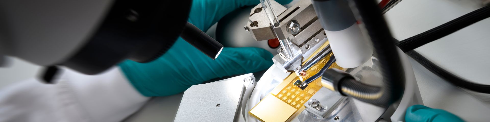
The Photonic Chip Pilot Line will enable production of Indium Phosphide (InP) photonic chips at 6-inch wafer scale. These chips are essential for breakthroughs in AI, quantum computing, medical diagnostics, and secure communications. You will contribute directly to their manufacturing and help bring cutting-edge technologies to life. As part of the EU-funded PIXEurope program, this pilot line will enable the transition to large-scale manufacturing.
The pilot line will be built at High Tech Campus Eindhoven, a major European photonics hotspot and home to the PhotonDelta ecosystem of startups, scale-ups, and research organizations. With access to top-tier facilities, deep expertise, and countless opportunities to learn, it is the ideal place for pioneers in this fast-evolving field. Whether you are an operator, engineer, or support specialist, your role will help shape the future of integrated photonics.
Discover the strategy
Boudewijn Docter: ‘We are not just conducting R&D; we are taking risks to build production capability and capacity for the demand in the near future. If we do not act now, we risk that we are not able to scale up tomorrow and Europe will lose its technological advantage in this critical field.’
Make impact, grow, and shape your future in tech
By joining the Photonic Chip Pilot Line, you will work at the forefront and actively contribute to the Netherlands’ ambition to lead in integrated photonics. To realize this, we seek professionals with an entrepreneurial mindset who understand that their role may look different in five years and who are open to a dynamic environment. Depending on the role, you’ll start on a state-of-the-art production line in a cleanroom environment, and later transition into shift operations. You'll have room to grow through technical training, collaboration with startups, tech companies and top universities, and career development with a close-knit team. This is your chance to shape the future of photonics.

'This Photonic Chip Pilot Line is a game-changer for Dutch companies and the future earning power and prosperity for the Netherlands. It is a critical part of a powerful ecosystem in photonic chips with which the Netherlands can distinguish itself worldwide.’
Become a pioneer in a fast evolving field
Why you should join the team
We seek professionals with an entrepreneurial mindset, excited to build something new.
From pilot to full factory scale
Why you should join the team
We have ambition to transfer the pilot to industry as a full-scale production facility.
Shape your future in tech
Why you should join the team
This is your chance to make real impact. For the Netherlands, for Europe, and for your own future.
Apply now and make your mark on our time
Frequently Asked Questions
Do you have questions about TNO’s Photonics Pilot Line Project? We have drawn up a selection of frequently asked questions.
The start of construction is planned for the 9th of March 2026. Construction will be happening on the High Tech Campus in Eindhoven, directly behind the existing SMART Photonics building.
At the start of the build in March 2026, a core team of specialists will start. As the factory construction progresses and becomes operational, the team will grow to about 40 employees.
Yes, you will receive a direct employment contract with TNO. The Photonic Chip Pilot Line is providing strong job security. After approximately five years, when the pilot line is fully operational, TNO plans to transfer it to industry ownership.
You will go through the full TNO onboarding process, including security screening. Depending on your role you will receive additional training at SMART Photonics facility and from various equipment suppliers. This truly is a collaborative ecosystem effort bringing together the best expertise from research institutions and industry partners.
SMART Photonics is one of our key partners and located right next door to TNO on the High Tech Campus in Eindhoven, literally within walking distance. Beyond SMART Photonics, we are working with several key partners in the photonics ecosystem. These include Photon Delta, Eindhoven University of Technology (TU/e), and AIXTRON, who will supply three reactors for the facility.
The photonics pilot line is to be build in Eindhoven, on the High Tech Campus. During the build, you will be based in TNO offices in Eindhoven. You will have regular meetings with your TNO team and remain under TNO supervision throughout.
Aside from the TNO onboarding and according to your role you will receive hands-on training at SMART Photonics' facility in Eindhoven to gain practical experience with industrial photonics manufacturing. You will also receive vendor training from various equipment suppliers, potentially traveling to their locations for one or two weeks to learn how to operate and maintain specialised tools.
This pilot line can best be compared to a startup. It will be a good fit for people who value being among the first employees, want to have real impact on the pilot line’s direction, and contribute to Europe's technological independence in photonics.
We understand that relocating is a major decision, especially regarding housing in Eindhoven's competitive market and perhaps finding (international) schools for your children. TNO has established policies and support systems to help you navigate the relocation process. We tailor this support based on the country of origin, familiarity with the Netherlands, and family composition. Read more: Terms and conditions of employment | TNO.
We are looking for candidates with hands-on industry experience rather than pure researchers or academics. The ideal profile is someone from the semiconductor or photonics industry (for example plasma engineers, lithography specialists, or etch/deposition technicians) who has practical cleanroom experience and wants to be part of building something from the ground up.
Contact us
-

Ilse de Graaf
Functie:Corporate Recruiter-
Standplaats:Eindhoven - Holst Centre
-
Email:Email Ilse
-
-
Brahim Dagdaoui
Functie:Corporate Recruiter‘You can achieve a lot at TNO if you take your chances’. Recruiter Brahim Dagdaoui has an eye for talent. It’s his job to make sure scientists find a place at TNO where they can blossom and work on groundbreaking innovations. He works for the units High Tech Industry and Mobility & Built Environment, where cool things are happening.’
-
Telefoon:+31 6 11 16 01 29
-
LinkedIn:Brahim on LinkedIn
-