Metrology and inspection concepts
The increasingly complex structures, 3D geometries, and new material combinations in state-ofthe-art chips gives rise to a huge demand for new metrology tools. Traditional methods do not suffice, for example because materials are optically opaque. That is the way TNO works on new metrology concepts: sometimes a new approach within an existing field, sometimes we even combine multiple approaches into one concept.
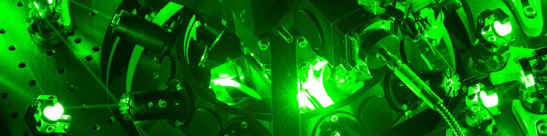
Optics
TNO develops knowledge within 5 technology lines:
- Spectroscopy identifies samples and characterizes matter using the wavelength of light.
- Fiber Optic Sensors measure chemical, biological, and industrial processes in demanding environments. This enables process control and optimization.
- Nano-Photonics develops integrated sensor systems for chemical, bio - chemical, and physical parameters. We also study the possibilities offered by promising metamaterials.
- Both high-end industrial production, such as lithography, and advanced scientific experiments, for example in astronomy, depend greatly on the availability of precise and robust monitoring systems. Metrology experts imagine, design, and develop such systems, including the technology needed to produce them.
- We offer complete calibration concepts for optical instruments that are unique in their application, such as satellite components
Acoustic metrology
TNO created a novel acoustic metrology method using GHz ultrasound waves to measure deeply buried subsurface features (>5μm). The concept consisted of a GHz acoustic transducer integrated above the tip of a custom-designed probe, which is then scanned across a sample. The method uses non-damaging solid-solid contact without the need for liquid coupling layers – in contrast to conventional acoustic microscopy. This allows for the use of much higher acoustic frequencies, hence higher on-axis resolutions. An experimental setup was built with a 4 GHz transducer and tested successfully on 1.5-2μm size features buried below a 5μm PMMA or 10μm SiO2 layer, respectively. These results demonstrated the feasibility of the new method, opening new opportunities for metrology and inspection applications
IR AFM
AFM-based methods are popular techniques to measure and check a broad range of material properties at the smallest length scales, especially in labs and universities. Similar to other scanning probe techniques, AFM traditionally relies heavily on operator experience to achieve good results. This can be attributed to poorly characterized tip shapes and complex resonant operating schemes in addition to strongly non-linear tip-sample interactions. TNO is developing unique operating modes, calibration methods, and data analysis algorithms. These all contribute to making AFM reach its high resolution material properties characterization. As a showcase, TNO is developing IR-AFM applications on imaging of resist-quality metrics such as chemical heterogeneity from blank resist or latent images. IR-AFM is a chemically specific imaging modality with nanometer resolution through IR spectroscopy applied with an AFM tip.
Contact us
-

William van Helden
Functie:Principal BD & Key Account Manager ASML-
Standplaats:Delft - Stieltjesweg
-
Email:Email William
-
LinkedIn:William on LinkedIn
-
-

Maarten van Es
Function not known-
Standplaats:Delft - Stieltjesweg
-
Email:Email Maarten
-
-

Olaf Kievit
Functie:Senior Business Developer-
Standplaats:Delft - Stieltjesweg
-
Email:Email Olaf
-
-

Sjoerd Oostrom
Function not known-
Standplaats:Delft - Stieltjesweg
-
Email:Email Sjoerd
-
Get inspired
Devices for detecting and measuring small particles