Thin-Film Electronics: Precision that accelerates
For more than 10 years, TNO’s experts at Holst Centre have been developing thin-film technology to enable batteries, photovoltaics, OLED lighting, OLED displays, imagers and much more. By combining and integrating a variety of technologies and processes, Holst Centre is uniquely qualified to demonstrate and qualify new device concepts and help industry partners realise state-of-the-art applications.
EXPERIENCE ON THE CUTTING EDGE
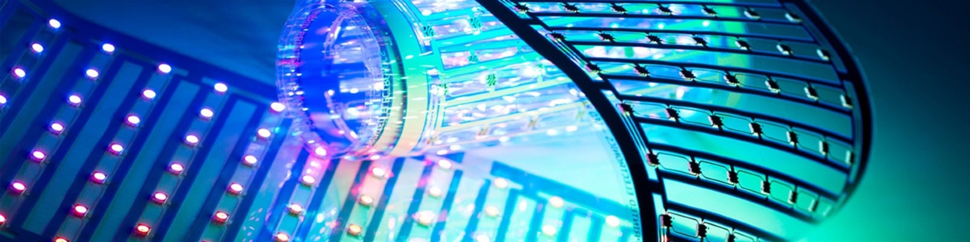
For industries that develop displays, medical imagers and bioelectronics, but also for those branches that provide energy conversion and storage, thin-film technology offers the form factor and functionality that manufacturers need. TNO at Holst Centre pushes the boundaries in individual technologies and in their integration, making use of a range of deposition and patterning technologies.
NEXT-GENERATION ALD
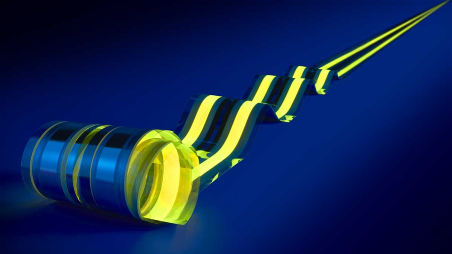
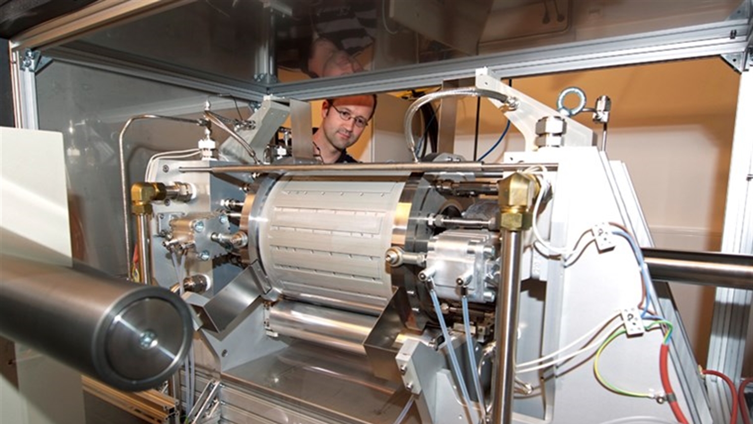
Atomic Layer Deposition (ALD) offers precise control and uniformity of film composition and thickness. TNO’s spatial ALD (s-ALD) solution adds much higher deposition rates and an atmospheric pressure process that does not require costly vacuum equipment.
TNO has successfully scaled up s-ALD to large areas in sheet-to-sheet and roll-to-roll equipment. The technology is ready for optimisation and integration into commercial production of solid-state batteries, photovoltaics, displays and semiconductor components.
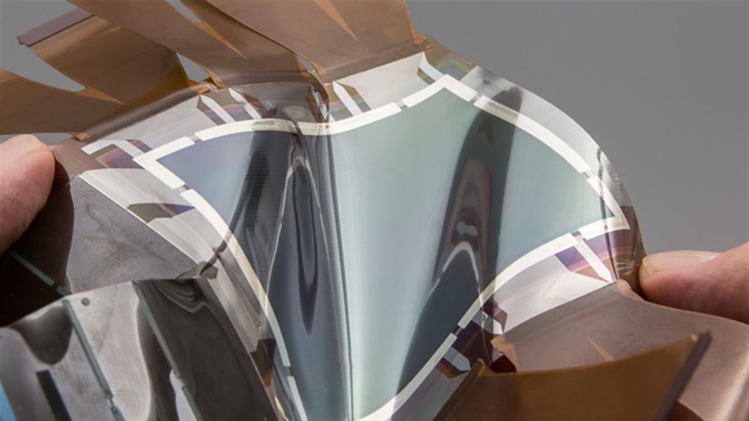
THIN-FILM TRANSISTOR TECHNOLOGY
TNO is a forerunner in oxide thin-film transistors (TFTs). These are primarily used for displays and imagers, but a host of other applications are possible. We have advanced TFT performance, for example by using s-ALD for semiconductor and dielectric layers.
SECURITY IN THE DIGITAL AGE
To address the need for heightened security, TNO has developed expertise in large-area, high-resolution optical sensors. These are ideal for under-display fingerprint and biometric detectors that protect against spoofing and security breaches. They deliver high resolution in sizes large enough for palm and four-finger scans and yet are thin, lightweight and (semi-)transparent, so can be integrated into various electronics and intelligent surfaces.
TNO also developed the world’s first high-resolution perovskite-based fingerprint sensor with over 80% EQE. Its near-infrared sensors can also be applied for biomedical imaging of the outer skin, giving access to measurement of various health parameters.
NEXT-GENERATION ULTRASOUND
Safe, radiation-free medical imaging is possible through ultrasound. However, current technology requires a highly skilled operator who is located at a healthcare centre. The technology also only offers a small field of view.
With our unique thin-film electronics, TNO at Holst Centre makes it possible to create large-area, flexible transducer arrays that will allow hands-free ultrasound systems that do not require a skilled operator. The ultrasound-on-foil technology allows thousands of individual transducers to be integrated into an adhesive patch. Such patches can be used, for example, for at-home monitoring of high-risk pregnancies and arterial plaque build-up.
FUTURE FOCUS
TNO at Holst Centre aims to continue to advance technology in healthcare. The same technology used to create foldable displays and semi-transparent imagers will be applied to innovative microfluidics, bioelectronics and potentially even brain/computer interfaces.
What’s more, TNO continues to invest in the energy domain, with the development of next-generation lithium-ion batteries, fuel cells and electrolysers.
Contact us
-

Auke Kronemeijer
Functie:Research Manager Thin-film electronicsAuke Jisk Kronemeijer is experienced in shaping and managing collaborative R&D programmes in the field of flexible & large area electronics. He currently leads the Thin-film electronics research group at TNO in Holst Centre working on technological applications in the fields of energy storage and health.
-
Standplaats:Eindhoven - High Tech Campus 25
-
Email:Email Auke
-
Get inspired
PITCCH event: Showcasing Open Innovation
Materials solutions

Hybrid printed electronics