Contamination control for semiconductor equipment
TNO is a specialist in contamination control for extreme ultraviolet lithography (EUV). We develop modules, research equipment, and strategies for the contamination control of EUV lithography scanners and materials and have been a trusted partner of ASML and Carl Zeiss in this regard for 20 years.
Leader in contamination control
We are specialists in contamination control research. We develop instrumentation and strategies for applications with the most challenging requirements in the High Tech Industry, including EUV lithography. The goal is to mitigate both particulate and molecular contamination. We have advanced facilities for the inspection and analysis of contamination, cleaning equipment, and setups to research the effect of EUV light and plasma. Our ultra-clean equipment is also suitable for validation of EUV masks.
Our contamination control infrastructure
TNO has expanded its research and development (R&D) infrastructure. This second EUV exposure setup including surface analysis equipment was put into operation in 2018. It is used for research into materials such as optics, reticles, and pellicles, in collaboration with various parties in the EUV lithography field, including materials suppliers, end users, and equipment developers.
Functionalities:
- The system accepts a variety of sample sizes, including standard EUV reticles with or without pellicles.
- EBL2 also has an XPS system that can analyse EUV masks and pellicles, including a functionality for the production of a ‘defect map’.
- Automated sample handling accepts SEMI-standard dual pods and maintains NXE compatibility for particle contamination on the back end.
- The system is suitable for exposure of samples to very high doses of EUV, and for returning the reticles for use in a wafer fab.
| Category | Specification |
|---|---|
| Optical power |
>1 W in 2% BW at 13.5 nm (‘IB’) (10 W in OoB ((10-20 nm )) at 3 kHz |
| Intensity | >1 W/mm2 IB in focus at 3 kHz |
| Cross-sectional optical focus | 1 - 30 mm diameter (adjustable power density) |
| Source frequency | 1 Hz - 10 kHz (default 3 kHz) |
| Sample size | Max. 152x152x20 mm (EUV mask + pellicle possible) |
| Dose control | <20 % with source feedback turned off |
| Continuous exposure time | >100 hours |
| In-vacuum analysis techniques | Ellipsometry and XPS |
Facility for exposure and analysis: EBL2
We have been researching the interaction between EUV and different materials since 2000. To facilitate the ASML power roadmap, a second facility was developed for EUV exposure and in-situ surface analysis, also known as EBL2. This system helps customers evaluate their materials and components for NXE-relevant EUV radiation and environmental factors so as to increase the service life and prevent contamination.
The EUV Beam Line 2
The main facility for EUV development is the EUV Beam Line 2 (EBL2). This integrated vacuum system consists of a vacuum chamber, in which to carry out the EUV exposures in a controlled environment, and an XPS for surface analysis. In this system, samples can be transported between the test environment and the XPS without disturbing the vacuum.
In the vacuum system of the EBL2, samples are exposed to EUV radiation for extended periods of time in a controlled, representative environment. An in-situ ellipsometer with imaging is available for real-time monitoring of exposure progress.
Contact us
-

Wilbert Staring
Functie:Director Business Development Quantum Technology-
Standplaats:Delft - Stieltjesweg
-
Email:Email Wilbert
-
-

Cor Rops
Functie:Senior Scientist Thermal and Fluidic EngineeringCor Rops graduated his studies Applied Physics in 1998 cum laude at the research group Fluid Mechanics at the TuDelft and started working for TNO early 1999. In 2004 he started in close collaboration with the TuDelft his PhD project on two phase flow and boiling at small structures, which he successfully finished in 2009. From this research he developed a method to realise stable flow boiling within microfluidic devices. After introduction in the high-tech industry, this method is now successfully applied in chip cooling for antenna arrays and power electronics for test equipment for electrical vehicles. Currently, other application areas are explored as well such as the data centre market and fuel cell industry.
-
Standplaats:Eindhoven - High Tech Campus 25
-
Email:Email Cor
-
-

Jacqueline van Veldhoven
Functie:Scientist"From sea mines to semiconductors, only TNO can do that!" Jacqueline van Veldhoven is a researcher in the nano-instrumentation department at TNO. She originally came to TNO to work on combating sea mines, but now has work that is closer to her PhD research: to find out how lithographic machines in the semiconductor industry can continue to produce cleanly.
-
Standplaats:Delft - Stieltjesweg
-
Email:Email Jacqueline
-
Get inspired
Quantum innovation projects
The qubit: there and back again
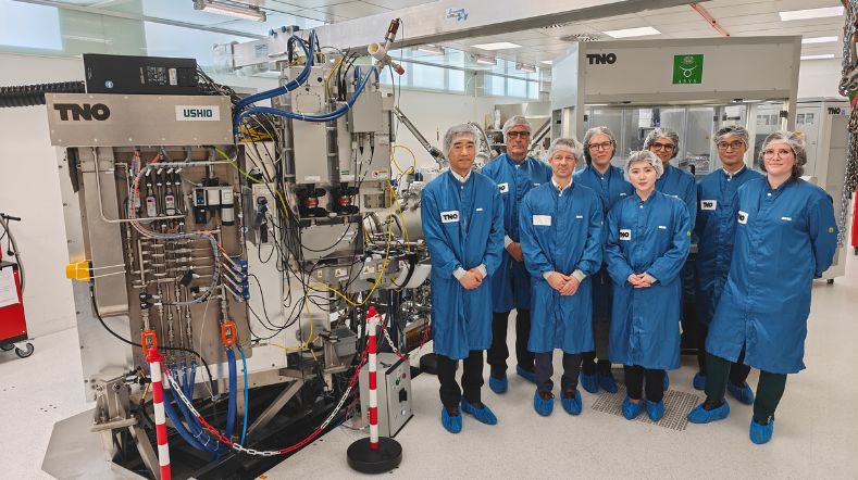
TNO and Ushio, a stable partnership in advancing EUV technologies
Quantum internet and quantum networks series 1.0

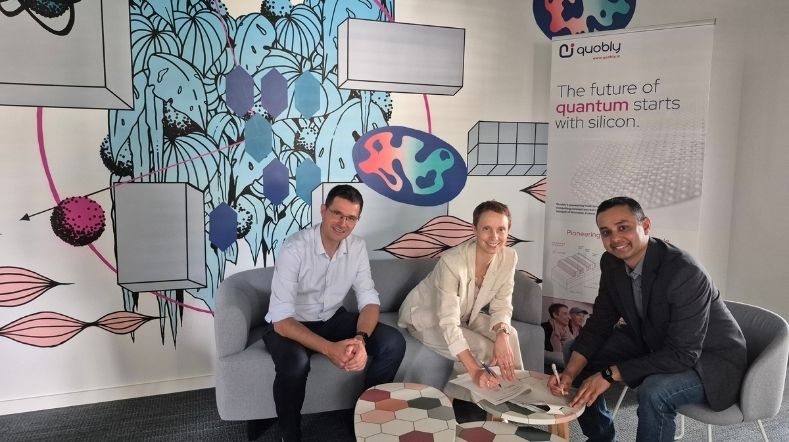
TNO and Quobly join forces to advance industrial-scale silicon quantum technology