Devices for detecting and measuring small particles
Modern technologies are used to measure and maintain microscopic surfaces, and keep them free of dirt. We measure defects with scanning probe microscopy and detect the smallest particles with our special scanner, the Rapid Nano.
Detecting small particles
In chip manufacture, it’s important that no particles end up on chips. Even the tiniest particle can make the product unusable. We therefore have a way of detecting 50-nanometre-sized particles using our special scanner, the Rapid Nano. This enables us to assess which working methods are as clean as possible and how they can be improved.
The Rapid Nano
The Rapid Nano is a relatively affordable tool that scans the complete reflective surface (e.g., EUV masks) in a shielded clean box. This is done at a speed of 100 cm2 per hour. The solution can then be integrated into the client’s process.
Rapid Nano Particle Scanner
The Rapid Nano is an affordable tool for particle inspection of EUV blank reticles and reticle substrates.
Fast and detailed
According to the latest standards, during the production process, semiconductor devices must not add more than one 50-nanometre particle per 10 cycles to a 15 x 15 cm mask. You can compare this with flying over the Netherlands in a fighter jet, looking for a tennis ball. And you want to have the results within a few hours. This calls for a fast and detailed method.
Know-how at TNO
We’ve been a leader in the field of particle detection for 10 years. We devise methods for reliably detecting and locating defects using our knowledge of optics, signal processing, vacuum technology, and ultra-clean handling.
Contact us
-

William van Helden
Functie:Principal BD & Key Account Manager ASML-
Standplaats:Delft - Stieltjesweg
-
Email:Email William
-
LinkedIn:William on LinkedIn
-
-
Olaf Kievit
Functie:Senior Business Developer-
Standplaats:Delft - Stieltjesweg
-
Email:Email Olaf
-
-

Sjoerd Oostrom
Function not known-
Standplaats:Delft - Stieltjesweg
-
Email:Email Sjoerd
-
-

Erik Schuring
Functie:Lead Researcher Materials Science-
Standplaats:Petten - Westerduinweg
-
Email:Email Erik
-
Get inspired
Towards low-cost, high-performance solar power for future space missions

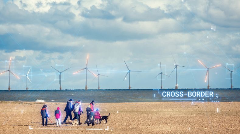
'The North Sea is crucial for the Netherlands, and that deserves wider recognition'
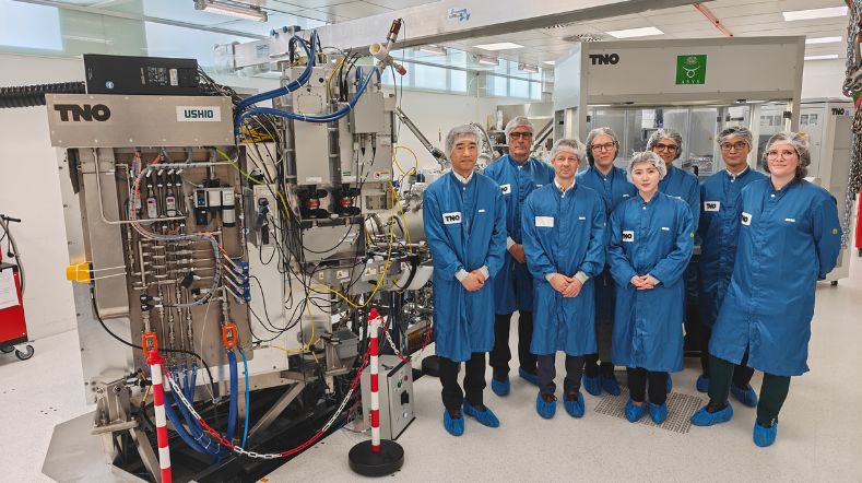
TNO and Ushio, a stable partnership in advancing EUV technologies
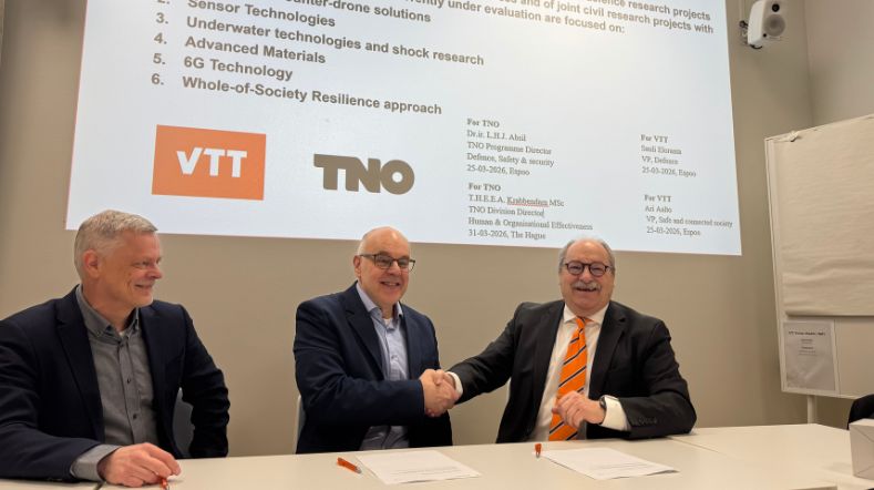
Closer cooperation between TNO and VTT (Finland) in the field of defense