A partnership built on the dream of EUV success
In the late 1990s, ASML was ready to follow its dream of revolutionizing the entire chip industry by developing machines based on EUV technology. To do that, it needed specialist competencies from outside its own knowledge branch. TNO’s multidisciplinary approach to finding solutions, and its own faith in the potential of EUV, made it a perfect partner to accompany ASML on this exciting voyage. It marked the start of a relationship that, more than a quarter-century on, is still as strong as ever.
Ever since its beginnings, ASML has operated on the cutting edge of technology. Despite the many skeptical viewpoints and slightly aided by a TNO study, it held strong in its belief that EUV technology was the key to taking lithography into the future. Where others chose different routes, ASML chased its dream by collaborating with experts from other disciplines to build the very first EUV lithography prototypes, the Alpha Demo Tools. Among the partners selected for this multiyear project were Philips, Carl Zeiss and TNO.
The theoretical potential of EUV lithography in semiconductor device fabrication was clear. The challenge, however, was turning this theory into a working tool. After all, to guarantee EUV scanner productivity and yield, it needed to operate with extreme precision inside a vacuum environment that remained ultra-clean. A feat that until then had proven unattainable. TNO was eager to apply its years of scientific work in aerospace and oil and gas, among other fields, to designing and building hardware for ASML’s Alpha Demo Tools and starting research lines, some of which are still active and relevant today.
Key developments
One piece of hardware TNO worked on for the project was the reticle handler, which needed to meet EUV’s extreme accuracy and cleanliness requirements. TNO developed a technique for placing the reticle using a pre-alignment sensor from the space industry. It involves using algorithms for measuring the position of satellites based on the pattern of the stars, enabling incredibly accurate alignment with the EUV scanner. The technology worked so well that these sensors are still used in today’s EUV systems. This was only one of several components in the EUV system that TNO worked on for ASML. The storage box, a vacuumized environment housing the reticle, had to be built to operate in compliance with the incredibly strict specifications for particles and reticle cleanliness. This time, TNO made use of its contamination and cleaning competence acquired in the space and high-tech industry.
A new technology will always run into new, yet unexplored challenges. For holding the reticles, for example, conventional wafer chucks, which rely on vacuum as a holding force, no longer sufficed since EUV lithography demands a vacuum environment. TNO teamed up with experts from Philips and Berliner Glas (now ASML Berlin) to design an electrostatic clamp that can keep reticles or wafers in position with incredible precision inside a vacuum environment.
Another technological innovation in the EUV scanner is the level sensor, a device designed by TNO and ASML for fast and accurate mapping of the wafer topography. TNO is still involved in the further development of the level and alignment sensors. Most recently, ASML adopted a concept for a new type of mirror control that TNO has developed for laser satellite communication. Both partners are once again working together on adapting the mirror to further improve the optics for the EUV source.
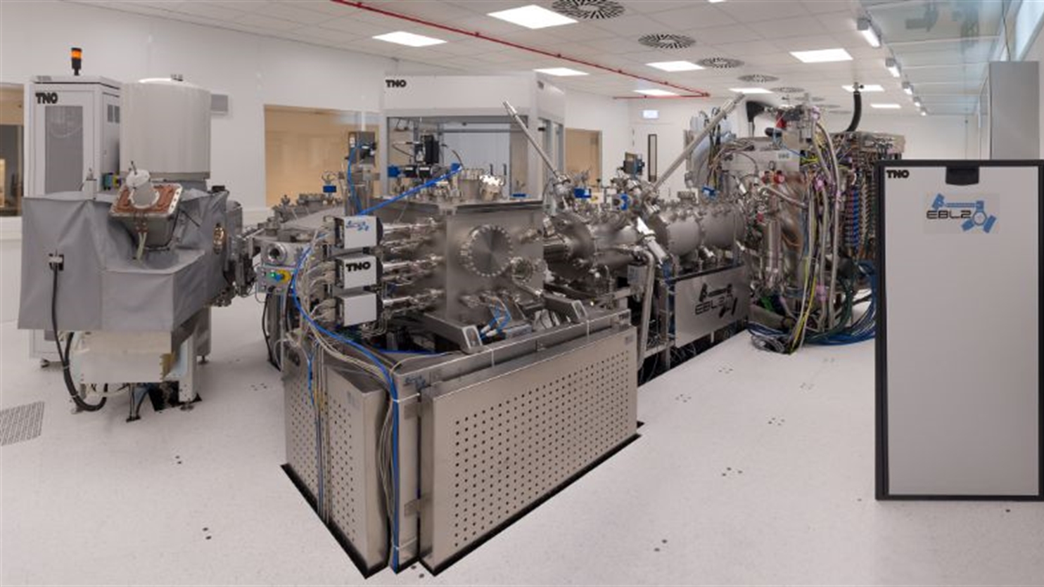
Other TNO innovations that have contributed to the success of ASML’s EUV lithography systems include the dynamic gas lock, the zero sensor and the wafer clamps. TNO now has its own highly advanced facilities like EBL-II, where ASML and its customers can measure, inspect and analyze contamination and cleaning equipment. Also, setups are in place to research the effect of EUV light on materials. It’s another testament to the strong bond that has grown over the years, whereby TNO is still able to support ASML with system improvements.
To measure is to know
“To measure is to know,” Lord Kelvin once famously said. But how can you know you’ve met the specifications of a technology that still needs to be proven? Here, TNO developed specialized measuring equipment to quantify these data. It turned out to be quite useful later on, when customers started using the EUV machines in the field and TNO was able to prove that ASML was by far the cleanest and fastest in terms of handling.
This organically led to a new competence domain within the project, contamination control, with which TNO continues to support ASML and its suppliers like Carl Zeiss until today. Particles, molecular contamination, gas flows impacting particle transport and thermal management, plasma effects - the field is still in flux.
Adding immersion to the equation
Besides ASML’s efforts to introduce EUV lithography, it helped customers move forward through innovations in DUV. To enable them to follow Moore’s Law, it introduced DUV immersion lithography. This technique involves adding a liquid medium between the final lens and the wafer to increase the refractive index, thus enhancing the photolithography resolution to achieve much finer feature sizes on the chip.
The problem at the time was containing and stabilizing the liquid within the immersion hood. The answer lay in two-phase flow, another domain where TNO had gained considerable knowledge through its ongoing R&D projects in the oil and gas industry. Of course, developing a two-phase flow system on such a tiny scale posed new challenges. TNO’s understanding of microfluidics helped to make it work. What’s more, adding immersion technology to the equation gave ASML and its customers more time to develop EUV lithography.
ASML and TNO continue to develop new immersion lithography systems together, intending to fulfill the industry demand to realize the optimum lithographic process for the different layers on the chips. After working on immersion technology together with ASML for almost two decades, TNO has applied the knowledge in other areas as well, such as micro-cooling. The next step is using the acquired knowledge to cool chips in data centers to save energy and prolong chip service life.
Driving industry forward
Like TNO, ASML approaches any new technology or idea by working in collaborative networks and isn’t afraid to exchange knowledge in the process. Throughout the EUV project, a sense of mutual understanding grew that the learnings could also be applied outside the lithography field to benefit other areas of industry. TNO has broadened its horizon enormously from working with ASML, not only from a technology perspective. In a practical sense, too, it has learned a great deal in terms of systems engineering and about the semiconductor industry in general. It’s partly thanks to ASML’s openness to share that TNO now supports several chip and equipment manufacturers across the world, but always with the interest of the Dutch industry in mind. TNO fulfilled an important role during the initial years of EUV lithography development to help realize the big dream. Even now that ASML has grown into the global market leader it is today, TNO continues to provide support in areas such as optics and contamination control. And whenever two technologies – such as acoustics and optics – need to be combined to discover new, innovative applications, TNO has the unique ability to compose a multidisciplinary team to get the job done.
The collaboration between ASML and TNO, which began in the late 1990s, is far from over. It’s as strong as when they first embarked on this journey. ASML’s continuous drive to innovate is a push for TNO to keep surprising with ideas that ASML hasn’t thought of, or technology combinations that haven't yet been combined in industry. And ASML knows that if a challenge can’t be solved at the monodisciplinary level, it can always call on TNO for a more multidisciplinary solution.
In return, the knowledge and expertise TNO has gained through its long partnership with ASML is vital in its aspirations to help Dutch parties in other parts of the semiconductor value chain move forward. By continuing to push each other forward, TNO and ASML can maintain their positions as key drivers for the economic ecosystem in the Netherlands and the global semiconductor industry.
Contact us
-
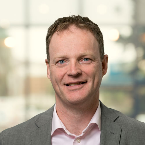
Rogier Verberk
Functie:Director Semicon & QuantumDr Rogier Verberk holds a PhD In experimental physics from Leiden University (2005). At TNO, the Dutch national Research and Technology Organisation, Rogier worked on EUV lithography with ASML and Carl Zeiss and became principal project manager.
-
Standplaats:Delft - Stieltjesweg
-
Email:Email Rogier
-
Get inspired
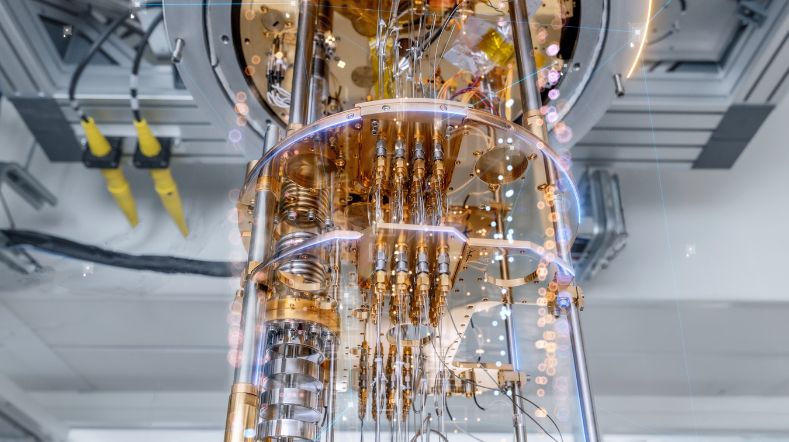
Quantum innovation projects
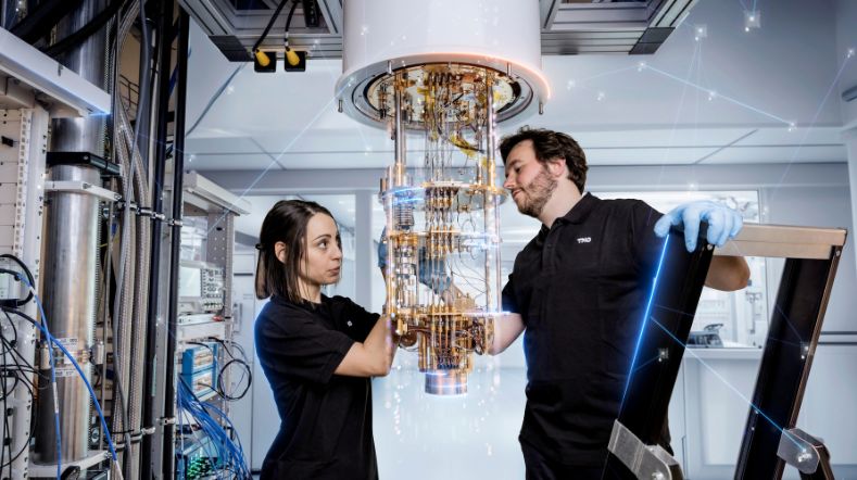
The qubit: there and back again
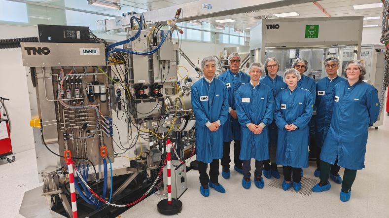
TNO and Ushio, a stable partnership in advancing EUV technologies
Quantum internet and quantum networks series 1.0

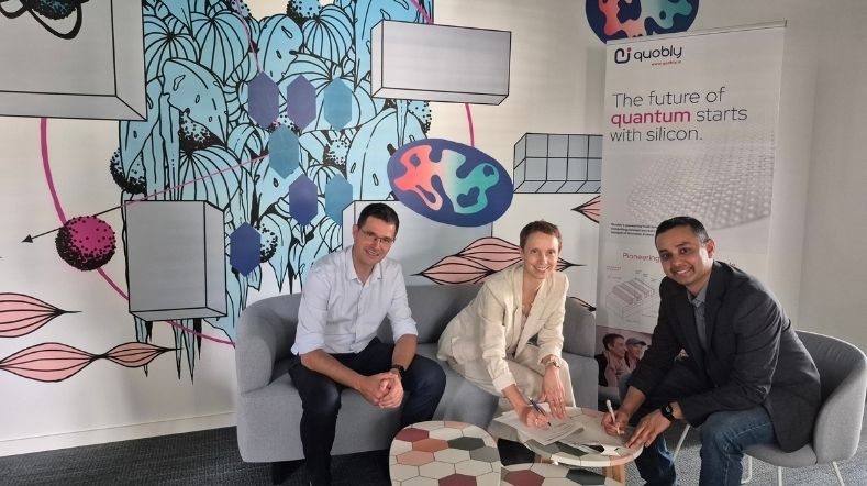
TNO and Quobly join forces to advance industrial-scale silicon quantum technology