R&D Scientist – Advanced Semiconductor Chip Packaging | Nijmegen
Want to make your mark on our time? Become a R&D Scientist – Advanced Semiconductor Chip Packaging at TNO in Nijmegen!
About this position
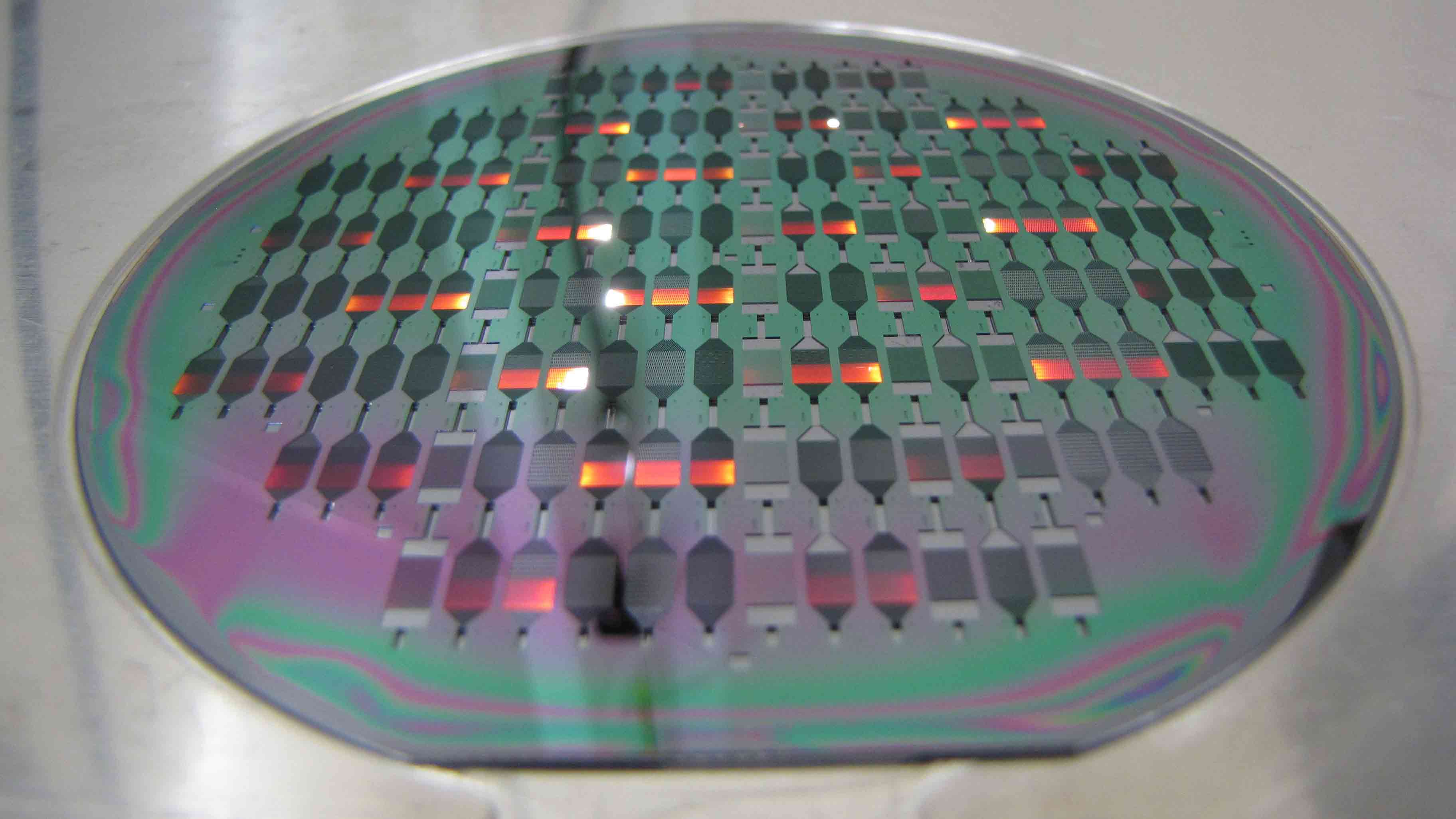
TNO is the Netherlands Organisation for Applied Scientific Research. As an independent research institute, TNO connects science and industry to accelerate innovation and translate knowledge into practical, scalable solutions. By combining deep technical expertise with a strong application focus, TNO supports companies and governments in addressing complex technological and societal challenges. Within the semiconductor domain, TNO plays a leading role in the development of advanced chip packaging technologies through the Chip Integration Technology Center (CITC). Under the CITC brand, TNO collaborates with industry leaders, materials suppliers, and equipment manufacturers to strengthen Europe’s position in semiconductor packaging and to enable the next generation of high-performance electronic systems. Through its Advanced Packaging Platform, TNO develops and scales innovative fan-out packaging technologies built on decades of expertise in large-area processing, thin-film electronics, and additive manufacturing. This platform combines advanced infrastructure, including a dedicated back-end lab in Nijmegen and state-of-the-art cleanroom facilities for thin-film and additive manufacturing processes at the Eindhoven campus.
What will be your role?
Within the Advanced Packaging Platform at CITC, you will contribute to the development of next-generation chip packaging technologies for demanding applications such as automotive radar systems and high-frequency RF and mmWave devices.
As Scientist Advanced Chip Packaging, you will be actively involved in the full development cycle of advanced packaging solutions, from design and realization to experimental validation and characterization. Your work will focus on enabling reliable and scalable chip packaging technologies that integrate different semiconductor materials such as CMOS and III-V devices.
You will work at the intersection of materials science, microelectronics, and advanced packaging technologies. In this multidisciplinary R&D environment, you will collaborate closely with experts in materials engineering, device fabrication, modelling, and system integration.
In this role, you will combine hands-on experimental work with thermomechanical modelling and device characterization. Your work will contribute to the development of manufacturable and reliable packaging solutions that can be translated into industrial applications.
You will also collaborate closely with industrial partners and customers, translating real-world technology challenges into concrete development activities and technology roadmaps.
Key responsibilities:
- Design, fabricate, and experimentally validate advanced chip packaging devices and processes;
- Develop and optimise advanced packaging technologies and process flows for next-generation semiconductor devices;
- Perform thermomechanical modelling and reliability analysis of chip packaging solutions;
- Carry out device characterization and experimental validation to evaluate packaging performance;
- Contribute to technology development, including the generation of intellectual property and new process innovations;
- Act as technical lead within collaborative R&D projects involving international industrial partners;
- Translate industrial challenges and customer requirements into practical technology development strategies.
What we expect from you
You are a hands-on researcher with a strong technical background and a deep interest in advanced semiconductor packaging technologies.
You bring:
- A PhD or MSc degree in Mechanical Engineering, Electrical Engineering, Materials Science, Physics, or a related scientific discipline;
- At least 5 years of experience in research and development within enabling technologies for advanced chip packaging;
- Hands-on experience with device fabrication, advanced packaging processes, or semiconductor manufacturing technologies;
- Experience with thermomechanical modelling and reliability analysis of semiconductor devices;
- Experience with device characterization and experimental validation methods;
- Experience contributing to or leading technical proposals and R&D projects with industrial partners;
- The ability to work effectively in multidisciplinary research teams;
- Strong communication skills in English, both written and spoken.
What we offer:
- A collaborative and high-performing research environment with experts in semiconductor packaging;
- The opportunity to contribute to the next generation of advanced chip packaging technologies for RF and mmWave applications;
- Close collaboration with leading industrial partners and technology suppliers;
- Access to state-of-the-art research and development facilities within TNO’s advanced packaging platform;
- A stimulating R&D environment focused on innovation, knowledge sharing, and technological impact.
What you'll get in return
Challenging and varied work with a real impact. And plenty of opportunities as, at TNO, you are in charge of shaping your career. We offer a gross monthly salary (based on your knowledge and experience), 8% holiday pay, a 13th month bonus of 8.33% and a flex budget (5.58% + € 180). In addition, you will be given every opportunity to develop yourself.
TNO offers optional employee benefits, enabling you to tailor your benefits package to match your personal situation. You may also expect:
- An extremely professional, innovative working environment where colleagues are leading experts in their field.
- The opportunity to attend courses, workshops and conferences, and to receive training and coaching based on your needs.
- 33 days annual leave on a full-time basis plus a flexible holiday (prorated) that can be used on a cultural, religious, or otherwise important day of your choosing.
- An employer working towards a respectful, inclusive, and equitable work environment where every employee can flourish, with various employee networks that foster connection and give advice.
- We offer a comprehensive and flexible mobility plan that also includes full compensation for public transportation for commuting and business travel[OPTIONAL] or a leased car.
- Great social events with your team and other TNO colleagues. That’s how you will get to know a lot of people really quickly.
- Flexible working hours, the possibility to work parttime (32 or 36 hours) and the possibility of working from home.
- Extensive relocation package for international candidates.
- A good pension scheme.
Read more about tailoring your benefits package.
TNO as an employer
At TNO, we innovate for a healthier, safer and more sustainable life. And for a strong economy. Since 1932, we have been making knowledge and technology available for the common good. We find each other in wonder and ingenuity. We are driven to push boundaries. There is all the space and support for your talent and ambition. You work with people who will challenge you: who inspire you and want to learn from you. Our state-of-the-art facilities are there to realize your vision. What you do at TNO matters: impact makes the difference. Because with every innovation you contribute to tomorrow’s world. Read more about TNO as an employer.
At TNO we encourage an inclusive work environment, where you can be yourself. Whatever your story and whatever unique qualities you bring to the table. It is by combining our unique strengths and perspectives that we are able to develop innovations that make a real difference in society. Want to know more? Read what steps we are taking in the area of diversity, equity and inclusion.
The selection process
Please apply before the 26th of April, 2026. The selection process comprises two interview rounds. In a final meeting we will discuss the terms of employment and your tailored benefits package. We aim to finalize the entire process within four weeks.
The selection process may include an online assessment and a reference check.
A certificate of Conduct (VOG) is required before starting a new job at TNO.
Has this job opening sparked your interest?
Then we’d like to hear from you! Please contact us for more information about the job or the selection process. To apply, please upload your CV and covering letter using the ‘apply now’ button.
More information about this vacancy?
-
Brahim Dagdaoui
Functie:Recruiter‘You can achieve a lot at TNO if you take your chances’. Recruiter Brahim Dagdaoui has an eye for talent. It’s his job to make sure scientists find a place at TNO where they can blossom and work on groundbreaking innovations. He works for the units High Tech Industry and Mobility & Built Environment, where cool things are happening.’
-
Telefoon:+31 6 11 16 01 29
-
LinkedIn:Brahim on LinkedIn
-
-
Pieter Debrauwer
Functie:Hiring managerPieter Debrauwer obtained his M.Sc degree in Aerospace Engineering in 2007 at TU Delft after which he started at TNO. He started in the field of fluid dynamics on lab on a chip application and 3D printing. Later moving to program management before becoming the research manager responsible for the department Equipment for additive manufacturing.
-
Standplaats:Eindhoven - High Tech Campus 25
-
Email:Email Pieter
-
LinkedIn:Pieter on LinkedIn
-
Posted by: #LI-BD1 Brahim Dagdaoui
Email: [email protected]