Semicon equipment lifetime
Advanced lithography equipment operates under challenging conditions. From extreme ultraviolet (EUV) photons, gas flows, plasma and high vacuums to particles and potential degradation. In order to ensure lithography equipment continues its precision work for the longest possible time, the TNO Semicon equipment lifetime research group offers bespoke lifetime studies and in-depth insight into equipment lifetime management.
Supporting industry innovation
Chip manufacturers are constantly innovating the materials and processes they use to advance their technology. TNO offers a Reticle Stack Assessment to assess the compatibility of new reticle materials with EUV lithography equipment. This fully independent and customised testing programme can recreate lifetime conditions at a highly accelerated pace. Of course, TNO protects all proprietary information about lithography materials and processes in strictest confidence.
TNO is ASML’s only offical partner for the Reticle Stack Assessment. After thorough investigation of the reticles (or other materials) sent for testing, TNO offers a complete report of material behaviour under EUV scanner-like conditions. When the reticle passes the assessment, ASML provides a waiver that enables chip manufacturers to use the reticle with the new materials in their EUV scanner.
Exploring beyond state-of-the-art
For more than 25 years, TNO has partnered with ASML and Carl Zeiss GmbH to test advancements in DUV and EUV lithography technology. From novel materials to new designs, we work closely with our partners to better understand how specific materials and components can affect productivity and yield and to further extend the lifetime of DUV and EUV lithography equipment. Our unique, state-of-the-art facilities offer a thorough perspective on how improvements and innovations impact the machine’s operability and longevity. We provide in-depth reporting that makes the impact of these innovations clear and tangible, and expert advice on the best approach.
Facilities for every need
TNO manages more than 20 different experimental facilities for testing and analysing lithography components. We are constantly improving our state-of-the-art EBL2 facility for EUV testing. We also offer unique plasma testing facilities, as well as (sub-)surface analysis afterwards. In many of these cases, we can ensure that a sample stays in vacuum between exposure and analysis. But perhaps our greatest added value is the expertise and knowledge we offer, which combines your test’s results with our 25 years of experience in equipment lifetime management. Our thorough investigations offer insights on a fundamental level, and precisely indicate the impact of materials on your machine.
Partnering for longevity
Manufacturers looking for assurance that their lithography machines will continue to run as needed for their entire expected lifetime turn to TNO for testing and advice. Our unique facilities and extensive knowledge in this domain are unmatched in the industry, and our independent way of working offers confidence and trust. Want to know more about our independent testing facilities? Contact us today.
Collaboration for advancement
TNO is actively engaged in a number of EU-funded research projects concerning advancements in EUV lithography and other related technologies. Although our work for clients is strictly confidential, we have published papers on our research. Please find some of these publications below.
J. van Veldhoven, C.C. Wu, A.J. Storm, M. van Putten, J.R. Meijlink, A.G. Ushakov, Measurements of ion fluxes in extreme ultraviolet-induced plasma of new EUV-beam-line 2 nanolithography research machine and their applications for optical component tests, Journal of Vacuum Science & Technology B 41 (1) (2023)
J. Stortelder, R. Ebeling, C. Rijnsent, M. van Putten, V. de Rooij-Lohmann, M. Smit, A. Storm, N. Koster, H. Lensen, V. Philipsen, K. Opsomer, D. Thakare, T. Feigl, P. Jaujok, First results of EUV-scanner compatibility tests performed on novel 'high-NA' reticle absorber materials, International Conference on Extreme Ultraviolet Lithography 2021 11854, 103-114 (2021)
J. van Veldhoven, A.S. Stodólna, A. Storm, J. van den Brink, N. Geerits, J. Vlaar, M. Dekker, A. Ushakov, Low-energy plasma source for clean vacuum environments: EUV lithography and optical mirrors cleaning, IEEE Transactions on Plasma Science 49 (10), 3132-3141 (2021)
Herman Bekman, Michael Dekker, Rob Ebeling, Jochem Janssen, Norbert Koster, Joop Meijlink, Freek Molkenboer, Kyri Nicolai, Michel van Putten, Corné Rijnsent, Arnold Storm, Jetske Stortelder, Chien-Ching Wu, Rory de Zanger, EBL2 an EUV (Extreme Ultra-Violet) lithography beam line irradiation facility, Proc. SPIE 11147, International Conference on Extreme Ultraviolet Lithography 2019, 1114706 (26 September 2019)
Jetske Stortelder, Arnold Storm, Veronique de Rooij-Lohmann, Chien-Ching Wu, Willem van Schaik, Compatibility assessment of novel reticle absorber materials for use in EUV lithography systems, Proc. SPIE 10957, Extreme Ultraviolet (EUV) Lithography X, 1095713 (26 March 2019)
Chien-Ching Wu, Edwin te Sligte, Herman Bekman, Arnold J. Storm, Michel van Putten, Maurice P.M. A. Limpens, Jacqueline van Veldhoven, Alex Deutz, EUV mask lifetime testing using EBL2, Proc. SPIE 10583, Extreme Ultraviolet (EUV) Lithography IX, 1058310 (19 March 2018)
Get inspired
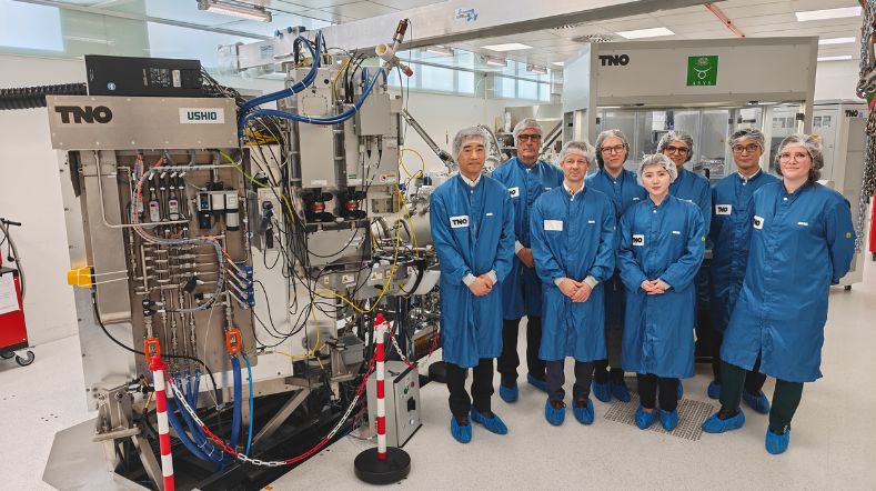
TNO and Ushio, a stable partnership in advancing EUV technologies

Quantum Circles: The Foundation for Europe’s Quantum Future
Quantum internet and quantum networks series 1.0

TNO and Quobly join forces to advance industrial-scale silicon quantum technology
Time setter story: Boudewijn Docter
