Nano instrumentation for ultra-clean lithography
Manufacturing Integrated Circuits requires ultra-clean and high-performance processes. Ultra-clean equipment with high demands on flow and thermal conditioning plays a major role in a manufacturer’s ability to achieve high yields. We help to develop and improve manufacturing equipment, so that it lasts longer and performs better.
When tech leaders such as ASML and Carl Zeiss encounter critical contamination issues, they turn to us for support. We have a team of 50 highly qualified Nano Instrumentation technologists and scientists who develop and assemble experimental set-ups on which they carry out experimental test programmes. We develop and own these set-ups, develop them together with our clients, or transfer full ownership to them.
Our aim is to prevent, diagnose, and remediate critical issues. We apply the principles of contamination control to design, build, and validate ultra-clean equipment for lithography. We continue to grow our extensive knowledge of molecular and particle contamination, vacuum and flow technology, and high-energy radiation, and apply this knowledge for our clients.
Take a look at the Nano Instrumentation expertise group
In-depth knowledge of Extreme Ultraviolet light (EUV)
At TNO, we use our knowledge of molecular and particle contamination in research on processes and the development of systems for the EUV lithography industry. In addition, we advise suppliers of the EUV lithography industry on clean production and how to achieve it. We apply our expertise in surface physics and physical chemistry in everything we do. That’s why we’ve been able to accelerate developments in all aspects of EUV. Below are some examples of our capabilities:
- metrology sensors for molecular contamination (MFIG)
- several experimental set-ups, including vacuum vessels
- hydrogen radical sensor based on heat flux sensors developed in house
- RapidNano (RN3) for fast inspection of EUV blanks. This is capable of detecting a single particle of some tens of nanometres on a 142 x 142 mm area.
- equipment to test molecular, chemical outgassing and resistance against hydrogen radicals and plasma
- plasma metrology equipment (RFEA, Langmuir probe)
- cleaning technology (wet cleaning, dry cleaning with or without plasma)
- particle sensor metrology (Fast Micro, PMC card, Part sense)
- EUV Beam Lines (EBL1 and EBL2) for optics lifetime research and research on EUV radiation effects on materials
- analysis systems such as optical microscopy (OM), Scanning Electron Microscope (SEM), plus material analysis with energy-resolved X-ray spectroscopy (SEM-EDX), X-ray Photoelectron Spectroscopy (XPS), ellipsometry, and Atomic Force Microscopy (AFM)
High-performance flow and thermal management
Semiconductor equipment and many other domains require high-performance flow and thermal management solutions. An example of a complex flow problem is keeping gasses and/or fluids apart even when surfaces that confine the gasses/fluids move fast relative to each other.
Examples of applications that involve complex flow problems:
- immersion hood equipment development
- development of a Spatial Atomic Layer Deposition system
- pressure and test wafers for ultraprecise (<1mW) determination of wafer heat loads and pressure distributions (1Pa)
- heating or cooling of semiconductor wafers within a specific time and with a specific homogeneity
- MicroFluidic Cooling of Automotive Electronics such as EV battery packs or 5G telecom driver chips
- flow and temperature slip (accommodation) properties of materials at reduced pressures
We have the domain expertise combined with the thermal and flow expertise to design and validate the above high-performance systems. We use simulation (CFD, FEM) and testing for this purpose. We hold a unique exclusive IP position in MicroFluidic cooling or evaporation.
Contact us
-

Frank Driessen
Function not known-
Standplaats:Delft - Stieltjesweg
-
Telefoon:+31 88 866 41 21
-
Email:Email Frank
-
Get inspired
TNO Semicon Innovation Day 2024
A partnership built on the dream of EUV success
SES-led EAGLE-1 onboards TNO and Airbus to deliver ground station for Quantum Key Distribution

TNO’s 2030 view: Ushering in the Quantum Era
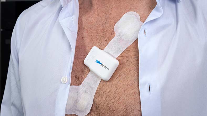
Monitoring your health using light: TNO designs wearable optical sensors